- 您现在的位置:买卖IC网 > Sheet目录3882 > PIC18F442T-E/ML (Microchip Technology)IC MCU FLASH 8KX16 EE A/D 44QFN
Micrel, Inc.
KSZ8864RMN
April 2012
11
M9999-043012-1.5
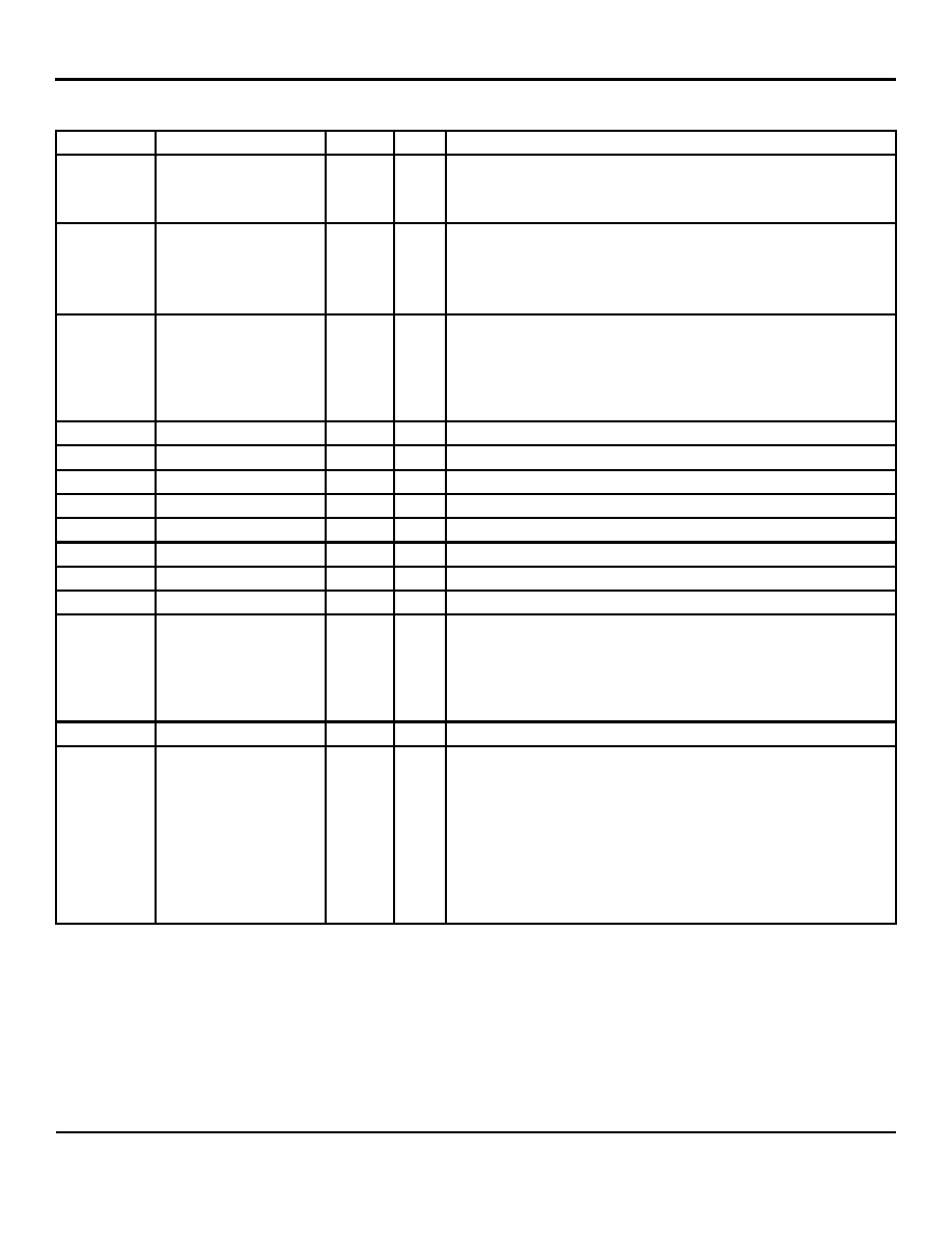
Pin Description (Continued)
Pin Number
Pin Name
Type
(1)
Port
Pin Function
(2)
26
SM3RXD2
IPD/O
3
MAC3 Switch MII receive bit 2 and Strap option:
PD (default) = disable back pressure;
PU = enable back pressure.
27
SM3RXD1
IPD/O
3
MAC3 Switch MII/RMII receive bit 1.
Strap option:
PD (default) = drop excessive collision packets;
PU = does not drop excessive collision packets.
28
SM3RXD0
IPD/O
3
MAC3 Switch MII/RMII receive bit 0.
Strap option:
PD (default) = disable aggressive back-off algorithm in half-duplex
mode;
PU = enable for performance enhancement.
29
SM3CRS
IPD/O
3
MAC3 Switch MII carrier sense.
30
GND
Ground with all grounding of die bottom.
31
SM3COL
IPD/O
3
MAC3 Switch MII collision detect.
32
SM4TXEN
IPD
4
MAC4 Switch MII/RMII transmit enable.
33
SM4TXD3
IPD
4
MAC4 Switch MII transmit bit 3.
34
SM4TXD2
IPD
4
MAC4 Switch MII transmit bit 2.
35
SM4TXD1
IPD
4
MAC4 Switch MII/RMII transmit bit 1.
36
SM4TXD0
IPD
4
MAC4 Switch MII/RMII transmit bit 0.
37
SM4TXC/SM4REFCLK
I/O
4
MAC4 Switch MII transmit clock:
Input: SW4-MII MAC mode clock.
Input: SW4-RMII reference clock, please also see the strap-in pin
P1LED1 for the clock mode and normal mode.
Output: SW4-MII PHY modes.
38
VDDIO
P
3.3V, 2.5V or 1.8V digital VDD for digital I/O circuitry.
39
SM4RXC
I/O
4
MAC4 Switch MII Receive clock:
Input: SW4-MII MAC mode.
Output: SW4-MII PHY mode.
Output: SW4-RMII 50MHz reference clock (the device is default clock
mode, the clock source comes from X1/X2 pins 25MHz crystal).
When set the device as normal mode (the chip’s clock source comes
from SM4TXC), the SM4RXC reference clock output should be
disabled by the register 87. Please also see the strap-in pin P1LED1
for the selection of the clock mode and normal mode.
发布紧急采购,3分钟左右您将得到回复。
相关PDF资料
PIC18LF4539T-I/ML
IC MCU FLASH 12KX16 EE A/D 44QFN
PIC18F452T-E/ML
IC MCU FLASH 16KX16 A/D 44QFN
PIC18F442-E/ML
IC MCU FLASH 8KX16 EE A/D 44QFN
PIC18F2539T-I/SO
IC MCU FLASH 12KX16 EE AD 28SOIC
PIC18F4439T-I/PT
IC MCU FLASH 6KX16 EE A/D 44TQFP
PIC16LF77T-I/ML
IC MCU FLASH 8KX14 A/D 44QFN
PIC16F74T-E/ML
IC MCU FLASH 4KX14 A/D 44QFN
PIC16F74-E/ML
IC MCU FLASH 4KX14 A/D 44QFN
相关代理商/技术参数
PIC18F442T-I/L
功能描述:8位微控制器 -MCU 16KB 768 RAM 34I/O RoHS:否 制造商:Silicon Labs 核心:8051 处理器系列:C8051F39x 数据总线宽度:8 bit 最大时钟频率:50 MHz 程序存储器大小:16 KB 数据 RAM 大小:1 KB 片上 ADC:Yes 工作电源电压:1.8 V to 3.6 V 工作温度范围:- 40 C to + 105 C 封装 / 箱体:QFN-20 安装风格:SMD/SMT
PIC18F442T-I/ML
功能描述:8位微控制器 -MCU 16KB 768 RAM 34I/O RoHS:否 制造商:Silicon Labs 核心:8051 处理器系列:C8051F39x 数据总线宽度:8 bit 最大时钟频率:50 MHz 程序存储器大小:16 KB 数据 RAM 大小:1 KB 片上 ADC:Yes 工作电源电压:1.8 V to 3.6 V 工作温度范围:- 40 C to + 105 C 封装 / 箱体:QFN-20 安装风格:SMD/SMT
PIC18F442T-I/PT
功能描述:8位微控制器 -MCU 16KB 768 RAM 34I/O RoHS:否 制造商:Silicon Labs 核心:8051 处理器系列:C8051F39x 数据总线宽度:8 bit 最大时钟频率:50 MHz 程序存储器大小:16 KB 数据 RAM 大小:1 KB 片上 ADC:Yes 工作电源电压:1.8 V to 3.6 V 工作温度范围:- 40 C to + 105 C 封装 / 箱体:QFN-20 安装风格:SMD/SMT
PIC18F4431-E/ML
功能描述:8位微控制器 -MCU 16KB 768 RAM 34 I/O RoHS:否 制造商:Silicon Labs 核心:8051 处理器系列:C8051F39x 数据总线宽度:8 bit 最大时钟频率:50 MHz 程序存储器大小:16 KB 数据 RAM 大小:1 KB 片上 ADC:Yes 工作电源电压:1.8 V to 3.6 V 工作温度范围:- 40 C to + 105 C 封装 / 箱体:QFN-20 安装风格:SMD/SMT
PIC18F4431-E/P
功能描述:8位微控制器 -MCU 16KB 768 RAM 34 I/O RoHS:否 制造商:Silicon Labs 核心:8051 处理器系列:C8051F39x 数据总线宽度:8 bit 最大时钟频率:50 MHz 程序存储器大小:16 KB 数据 RAM 大小:1 KB 片上 ADC:Yes 工作电源电压:1.8 V to 3.6 V 工作温度范围:- 40 C to + 105 C 封装 / 箱体:QFN-20 安装风格:SMD/SMT
PIC18F4431-E/P
制造商:Microchip Technology Inc 功能描述:IC 8BIT FLASH MCU 18F4431 DIP40
PIC18F4431-E/PT
功能描述:8位微控制器 -MCU 16KB 768 RAM 34 I/O RoHS:否 制造商:Silicon Labs 核心:8051 处理器系列:C8051F39x 数据总线宽度:8 bit 最大时钟频率:50 MHz 程序存储器大小:16 KB 数据 RAM 大小:1 KB 片上 ADC:Yes 工作电源电压:1.8 V to 3.6 V 工作温度范围:- 40 C to + 105 C 封装 / 箱体:QFN-20 安装风格:SMD/SMT
PIC18F4431-E/PT
制造商:Microchip Technology Inc 功能描述:IC 8BIT FLASH MCU 18F4431 TQFP44